S R Flip FLop
SR Flip Flop
Flip flop is a term which comes under digital electronics, and it is an electronic component which is used to store one single bit of the information.

Diagrammatic Representation of Flip Flop
Since Flip Flop is a sequential circuit so its input is based upon two parameters, one is the current input and other is the output from previous state.It has two outputs, both are complement of each other. It may be in one of two stable states, either 0 or 1.
What is SR Flip Flop?
It is a Flip Flop with two inputs, one is S and other is R. S here stands for Set and R here stands for Reset. Set basically indicates set the flip flop which means output 1 and reset indicates resetting the flip flop which means output 0. Here clock pulse is supplied to operate this flop flop, hence it is clocked flip flop.
Construction of SR Flip Flop
We can construct SR flip with two ways, one is with 2 NOR Gates + 2 AND Gates and other is with 4 NAND Gates.

Ways to Construct SR Flip Flop


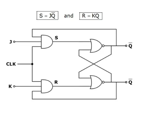
SR Flip Fop using two NOR and two AND Gates
Working of SR Flip Flop
- Case 1: Let’s say, S=0 and R=0, then output of both AND gates will be 0 and the value of Q and Q’ will be same as their previous value, i.e, Hold state.
- Case 2: Let’s say, S=0 and R=1, then output of both AND gates will be 1 and 0, correspondingly the value of Q will be 0 as one of input is 1 and it is a NOR gate so it will ultimately gives 0, hence Q gets 0 value, similarly Q’ will be 1.
- Case 3: Let’s say, S=1 and R=0, then output of both AND gates will be 0 and 1, correspondingly the value of Q’ will be 0 as one of input to NOR gate is 1, so output will be 0 ultimately and this 0 value will go as input to upper NOR gate, and hence Q will become 1.
- Case 4: Let’s say, S=1 and R=1, then output of both AND gates will be 1 and 1 which is invalid, as the outputs should be complement of each other.
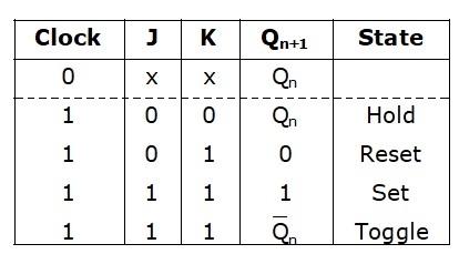
Truth Table of SR Flip Flop

Here, S is the Set input, R is the reset input,Qn+1 is the next state and State tells in which state it enters
J K Flip Flop
The JK Flip-Flop is a refinement of the S-R flipflop in which the S-R type’s indeterminate (invalid) state is defined.
JK Flip Flop is one of the most used flip-flops in digital circuits. The universal flip flop has two inputs, ‘J’ and ‘K.’ The JK Flip Flop is a gated SR Flip-Flop with a clock input circuitry that prevents the illegal or invalid output when both inputs S and R are equal to logic level “1.”

Comments
Post a Comment